How to Choose the Right Surface Finish for Your PCB

Electromagnetic Interference and Compatibility
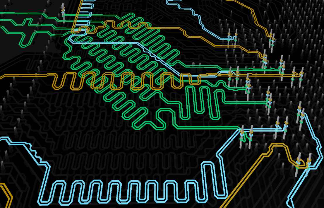
The first factor to focus on in high speed PCB design guidelines is EMI. EMI is nothing but electromagnetic energy that interferes with another electronic component or its path. This can also be a self-circuit disturbing noise. Electromagnetic compatibility of the device does not generate noise or has the ability to work without being interfered with by other electronic components.The third factor to focus on in high speed PCB design guidelines is the transmission lines. Transmission lines are generally micro-strip or strip lines. Microstrip patch lines are the traces that are on the outer layers with one reference plane under it whereas strip lines are the ones with dielectric and ground planes on both sides. If the signal wavelength and length of the traces are the same then these considerations have to be taken on the transmission line. The main dimensions of the transmission line considerations are the length of the trace the width of the trace, the trace thickness, and dielectric thickness that a PCB designer should consider and for the circuit designer, the considerations are the wavelength, Velocity of the signal, a combination of several dielectrics and the frequency.
Signal Speed and Propagation Delay: The speed of the signal from source to destination is called signal speed. The propagation delay is nothing but the time taken by the signal to reach the destination, this is also dependent on the speed of the strip line. These are used in applications where the timing, differential pair signals, and clock skew requirements are needed. Impedance: Another main factor of the transmission line is the characteristic impedance. The signal path or the signal change consists of a source, trace, vias, sync, or any connector. If the characteristic impedance changes, then the reflections happen on the transmission line. The sync has usually a high impedance input, therefore the following terminations are followed in PCB design. They are Series termination, Parallel termination, Thevenin termination, and AC termination.
Clock Signals
The second factor to focus on in high speed PCB design guidelines is the clock signal. The frequency domain of the clock signal is generally a square wave but it is very difficult to achieve and the signal going to peak voltage cannot be perfect square. The signal takes some time to reach the peak and come back to the fall state. This shape looks like a trapezoidal shape. Therefore the specification of driven devices should match the slew rate.The fourth factor to focus on in PCB design guidelines for high speed is the crosstalk. The Interference between two parallel or nearby routed lines is called crosstalk. The source lines and victim lines are couples with capacitive or inductive coupling and it induces a forward or a reverse current in the victim’s trace. The crosstalk in the strip line environment tends to cancel each other whereas in the microstrip line, they tend to undergo capacitive coupling.
To avoid cross-talk the adjacent traces are routed apart two times the width of the trace. Cross-talk in high-speed signal design can happen in two ways. The forward cross-talk traverses in the same direction as the source line as the length increases and the crosstalk increases concerning dV/dt. The reverse crosstalk increases when the amplitude is higher.The fifth factor to focus on in PCB design guidelines for high speed is the differential signals. Differential pairs of signals in each trace are equal but opposite in magnitude and opposite in direction. The Electromagnetic field tends to cancel each other concerning ground or reference path. To achieve this the trace length is equal to match the propagation delay. If the signal is radiated in both the traces then even the sensitive receiver does not identify it. This design constraint has to be matched by routing the traces close to each other.


Differential Signal Spacing
In high speed board design guidelines, differential signal spacing is a routing parameter that cannot be ignored. The spacing constraints for the differential signal routing for similar signals and inter-differential signals are also equally important. This is determined by the trace width of the signal. The space between a signal to signal is 8mils if the signal trace width is 6 mil, in this case, the space for any keep-out signal is determined by 5 times the signal distance. In this case, we weed 30 mils in the inter-pair keep-out area. If any one of the signals is a high-speed signal or clock skew or periodic signal then 50 mils distance is kept for the safer side.The sixth factor to focus on in PCB design guidelines for high speed is the return path.
Any electrical circuit should always be in a closed loop to function. The position of the source, sync, trace of the signal line, return path, cut in-ground, split in-ground, bridging component, or connector can influence a lot of loop area and return path.

Trends And Challenges In PCB Manufacturing For 2024
Understanding the Importance of X-ray in PCB Assembly